Introduction to Embedded Systems :: CSCI 255
Lab Assignments
Lab 3 -- Save the Island
HOME SYLLABUS HOMEWORK LABS LINKS NOTES
|
The goal of this assignment is introduce you to programming in assembly language on the MSP430 microcontroller. You will learn how to use port Port 1 & 2. You will gain experience using assembly language to create nested loops, conditional branches, and perform bit operations. Part 1 – CountdownYou need to create a count down timer. The timer should start at a value of 108 (decimal) and count down towards 0. The current value of the timer should be displayed in binary using LEDs. P2.0 is the least significant bit. An LED should be lit if its corresponding bit position in the binary representation of the timer's value is currently 1. The LEDs correspond to port 2 pins P2.0 (LSB), P2.1, ..., P2.5 (MSB). *** Make sure that you close the circuit correctly: Ground your circuit with the MSP430 *** Part 2 – Blow up the IslandOnce the timer reaches zero, stop the count down. Flash all 8 LEDs on and off several times a second. At the same time as the flashing LEDs, cause a buzzer to sound. The flashing and beeping continues forever (or until you unplug the board).
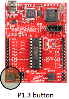
Part 3 – Now Save the IslandIf button P1.3 is pushed when the timer reaches zero, the timer should reset to 108 (Decimal) and start counting down again (without flashing all the LEDs or beeping). You will need to SET the button by using the instruction bis.b #BIT3, &P1REN
Port 1: Digital I/O Description (Ch7)Port P1 input, P1IN: reading returns the logical values on the inputs if they are
configured for digital input/output. This register is read-only and volatile. It does not
need to be initialized because its contents are determined by the external signals. Port P1 output, P1OUT: writing sends the value to be driven to each pin if it is
configured as a digital output. If the pin is not currently an output, the value is stored in
Digital Input, Output, and Displays 209
a buffer and appears on the pin if it is later switched to be an output. This register is not
initialized and you should therefore write to P1OUT before configuring the pin for Port P1 direction, P1DIR: clearing a bit to 0 configures a pin as an input, which is the
default in most cases.Writing a 1 switches the pin to become an output. This is for
digital input and output; the register works differently if other functions are selected Port P1 resistor enable, P1REN: setting a bit to 1 activates a pull-up or pull-down
resistor on a pin (like the P1.3 button). Pull-ups are often used to connect a switch to an input as in
the section "Read Input from a Switch" on page 80. The resistors are inactive by Port P1 selection, P1SEL: selects either digital input/output (0, default) or an alternative function (1). Further registers may be needed to choose the particular function. Button Example: How to make P1.3 work in Pseudo-code
Submission:1 - Have each part of the lab checked out by Matt, Clint or Damian by showing your code, flashing your code to the board, and display working circuit. 2 - Print your final (Part 3) code with the following header: /*************************************************** 3 - Make sure you have a well commented code 4 - Turn it in to Matt or Clint
Copyright © 2011 by Keith Vertanen. |
Montana Tech --
College of Letters, Science &
Professional Studies -- Computer Science
Department
All Rights Reserved and Copyright
© 2013 by Damian Valles